lobal PCB Samples Service Supplier
Whenever the urgent, we could make it.

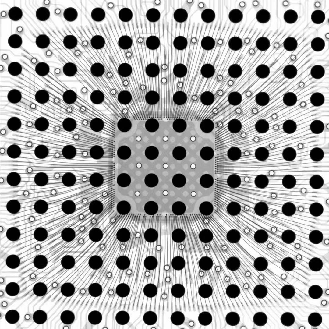
BGA芯片X-ray检测效果

BGA(Ball Grid Array)是一种常见的集成电路封装类型,它具有许多小球形焊盘,通常位于芯片的底部。由于这些小球很小且紧密排列,因此对于BGA焊接的质量和连接状态进行检测是至关重要的。X射线(X-ray)检测是一种用于BGA检测的常见方法,它可以提供非破坏性的内部图像,帮助评估焊接质量。
以下是关于BGA X-ray检测的一些关键点:
非破坏性检测: X-ray检测是一种非破坏性测试方法,可以在不影响BGA焊点的情况下查看焊点和连接状态。
焊点质量: X-ray可以揭示焊点的质量,包括焊料的均匀性、焊盘与焊球之间的连接是否牢固,以及是否存在焊接缺陷(如冷焊、干焊等)。
焊接间隙: X-ray可以检测焊盘和芯片之间是否存在过大或过小的间隙,帮助确定焊接的准确性。
位置偏移: X-ray可以显示焊球的位置是否与焊盘对齐,以防止焊球偏移或错位。
内部结构: 除了焊点质量,X-ray还可以提供有关BGA内部结构的信息,如是否存在空腔、内部线路连接等。
检测要求: BGA的小尺寸和紧密排列可能需要高分辨率的X-ray系统,以便准确检测细微的焊接问题。
操作注意事项: 在进行X-ray检测时,需要遵循安全操作规程,以确保操作人员和环境的安全。同时,设备的校准和正确设置也是确保测试结果准确的关键。
总之,BGA X-ray检测是一种常用于评估焊接质量和连接状态的非破坏性方法。它对于保障电子产品的质量和可靠性具有重要作用,尤其是在高密度封装中。
BGA soldering in detail:
Certainly! BGA (Ball Grid Array) soldering is a technique used to attach BGA packages to printed circuit boards (PCBs) or substrates.
BGA is a type of surface mount packaging for integrated circuits (ICs) in which the connections between the IC and the PCB are made
via an array of small solder balls or bumps located on the underside of the IC package.
Here's a detailed explanation of BGA soldering:
1. BGA Package Structure: BGA packages consist of an IC mounted on a small substrate, often made of ceramic or organic materials.
On the underside of the substrate, there is an array of solder balls or bumps arranged in a grid pattern.
These balls serve as the electrical connections between the IC and the PCB.
2. PCB Preparation: To begin the soldering process, the PCB is prepared by applying solder paste to the pads where the BGA package
will be attached. The solder paste is a mixture of solder particles and flux that is applied in a precise pattern on the PCB pads.
3. Placement: The BGA package is precisely aligned and placed onto the solder paste-covered pads on the PCB. The solder balls on
the package must align perfectly with the corresponding pads on the PCB to ensure proper connections.
4. Reflow Soldering: The PCB with the BGA package is then passed through a reflow oven. In the reflow oven, the temperature is
carefully controlled to heat the entire assembly to a point where the solder paste melts and flows, creating a reliable solder joint.
The temperature is then reduced to solidify the solder, forming a secure electrical connection.
5. Inspection: After the soldering process, the PCB assembly goes through an inspection phase. This can include visual inspection,
X-ray inspection, and other methods to ensure that all solder joints are uniform and without defects. X-ray inspection is particularly
important for BGA components because the solder connections are not visible from the surface.
6. Rework: In cases where solder joints are found to be defective or if there are issues with the initial soldering, rework may be required.
This involves removing the BGA package, cleaning the pads, applying fresh solder paste, and reattaching the BGA package.
Rework requires precision and care to avoid damaging the components.
7. Testing: Once the BGA component is securely soldered, the PCB assembly undergoes functional testing to ensure that all connections
are electrically sound, and the circuit functions as intended.
BGA soldering is a widely used technique in electronics manufacturing due to its compact design, high pin count, and reliable electrical
connections. It is commonly found in a wide range of electronic devices, from consumer electronics to aerospace applications. However,
it requires specialized equipment and expertise to ensure successful soldering, inspection, and quality control.
24 Hours Customer Service Hotline
+8613554998058-Danny
Send us email please
admin@tuopx.com